Keywords: UV laser pulses, nanostructuring, simulations, molecular dynamics
Acknowledgements. The reported study was supported partially by the Ministry of Education and Science of Russia, research agreement No.14.578.21.0197 (RFMEFI57816X0197, by RFBR grant No. 14-29-07227 OFI-M, and the Government of the Russian Federation The reported study was supported partially by the Ministry of Education and Science of Russia, research agreement No.14.578.21.0197 (RFMEFI57816X0197, by RFBR grant No. 14-29-07227 OFI-M, and the Government of the Russian Federation Grant No. 074-U01, and DFG grants IV 122/1-1, IV 122/1-2, and IH 17/18-1. The authors acknowledge the Lichtenberg Super Computer Facility (Darmstadt, Germany) team for the technical support provided for super large scale parallel simulations.
References
1. Chichkov B.N., Momma C., Nolte S., von Alvensleben F., Tünnermann A. Femtosecond, picosecond and nanosecond laser ablation of solids.
Applied Physics A, 1996, vol. 63, pp. 109–115. doi:
10.1007/bf01567637
2. Gattass R.R., Mazur E. Femtosecond laser micromachining in transparent materials.
Nature Photonics, 2008, vol. 2, pp. 219–225.doi:
10.1038/nphoton.2008.47
3. Vorobyev A.Y., Guo C. Direct femtosecond laser surface nano/microstructuring and its applications.
Laser and Photonics Reviews, 2013, vol. 7, pp. 385–407. doi:
10.1002/lpor.201200017
4. Lin B., Elsayed-Ali H.E. Temperature dependent reflection electron diffraction study of In(1 1 1) and observation of laser-induced transient surface superheating.
Surface Science, 2002, vol. 498, no. 3, pp. 275–284.doi:
10.1016/s0039-6028(01)01764-2
5. Siwick B.J., Dwyer J.R., Jordan R.E., Miller R.J.D. An atomic-level view of melting using femtosecond electron diffraction.
Science,2003, vol. 302, no. 5649, pp. 1382–1385. doi:
10.1126/science.1090052
6. Sokolowski-Tinten K., Blome C., Blums J., Cavalleri A., Dietrich C. et. al. Femtosecond X-ray measurement of coherent lattice vibrations near the Lindemann stability limit.
Nature, 2003, vol. 422, no. 6929, pp. 287–289.doi:
10.1038/nature01490
7. Ivanov D.S., Zhigilei L.V. Kinetic limit of heterogeneous melting in metals.
Physical Review Letters,2007, vol. 98, no. 19, art. 195701. doi:
10.1103/physrevlett.98.195701
8. Lin Z., Leveugle E., Bringa E.M., Zhigilei L.V. Molecular dynamics simulation of laser melting of nanocrystalline Au.
The Journal of Physical Chemistry C, 2010, vol. 114, no. 12, pp. 5686–5699.doi:
10.1021/jp909328q
9. Ivanov D.S., Lin Z., Rethfeld B., O'Connor G.M., Glynn Th.J., Zhigilei L.V. Nanocrystalline structure of nanobump generated by localized photoexcitation of metal film.
Journal of Applied Physics,2010, vol. 107, no. 1, pp. 013519.doi:
10.1063/1.3276161
10. Pronko P.P., Dutta S.K., Squier J., Rudd J.V., Du D., Mourou G. Machining of sub-micron holes using a femtosecond laser at 800nm.
Optics Communications, 1995, vol. 114, no. 1-2, pp. 106–110. doi:
10.1016/0030-4018(94)00585-i
11. Koch J., Korte F., Bauer T., Fallnich C., Ostendorf A., Chichkov B.N. Nanotexturing of gold films by femtosecond laser-induced melt dynamics.
Applied Physics A, 2005, vol. 81, no. 2, pp. 325–328. doi:
10.1007/s00339-005-3212-6
12. Hwang D., Ryu S.-G., Misra N., Jeon H., Grigoropoulos C.P. Nanoscale laser processing and diagnostics.
Applied Physics A, 2009, vol. 96, no. 2, pp. 289–306. doi:
10.1007/s00339-009-5207-1
13. Huber C., Trügler A., Hohenester U., Prior Y., Kautek W. Optical near-field excitation at commercial scanning probe microscopy tips: a theoretical and experimental investigation.
Phys. Chem. Chem. Phys., 2014, vol. 16, no. 6, pp. 2289–2296. doi:
10.1039/c3cp51730f
14. Ivanov D.S., Zhigilei L.V. Combined atomistic-continuum modeling of short-pulse laser melting and disintegration of metal films.
Physical Review B, 2003, vol. 68, no. 6, art. 064114. doi:
10.1103/physrevb.68.064114
15. Anisimov S.I., Kapeliovich B.L., Perel’man T.L. Electron emission from metal surfaces exposed to ultrashort laser pulses. Journal of Experimental and Theoretical Physics, 1974, vol. 39, no. 2, pp. 375–377.
16. Leveugle E., Ivanov D.S., Zhigilei L.V. Photochemical spallation of molecular and metal targets: molecular dynamic study.
Applied Physics A, 2004, vol. 79, no. 1, pp. 1643–1655. doi:
10.1007/s00339-004-2682-2
17. Zhigilei L.V., Lin Z., Ivanov D.S. Atomistic modeling of short pulse laser ablation of metals: connections between melting, spallation, and phase explosion.
The Journal of Physical Chemistry C, 2009, vol. 113, no. 27, pp. 11892–11906.doi:
10.1021/jp902294m
18. Ivanov D.S., Lipp V.P., Rethfeld B., Garcia M.E. Molecular-dynamics study of the mechanism of short-pulse laser ablation of single-crystal and polycrystalline metallic targets.
Journal of Optical Technology, 2014, vol. 81, no. 5, pp. 250–253. doi:
10.1364/jot.81.000250
19. Ivanov D.S., Lipp V.P., Blumenstein A., Veiko V.P., Yakovlev E.B. et. al. Experimental and theoretical investigation of periodic nanostructuring of Au with UV laser near the ablation threshold.
Physical Review Applied, 2015, vol. 4, no. 6, art. 064006. doi:
10.1103/physrevapplied.4.064006
20. Ivanov D.S., Lipp V.P., Blumenstein A., Veiko V.P., Yakovlev E.B., Roddatis V.V., Garcia M.E., Rethfeld B., Ihlemann J., Simon P. Analysis of periodic nanostructures formation on a gold surface under exposure to ultrashort laser pulses near the melting threshold. Scientific and Technical Journal of Information Technologies, Mechanics and Optics, 2015, vol. 15, no. 6, pp. 984–999. (in Russian).
21. Corkum P.B., Brunel F., Sherman N.K., Srinivasan-Rao T. Thermal response of metals to ultrashort-pulse laser excitation.
Physical Review Letters,1988, vol. 61, no. 25, pp. 2886–2889.doi:
10.1103/physrevlett.61.2886
22. Demsar J., Averitt R.D., Ahn K.H., Graf M.J., Trugman S.A., Kabanov V.V., Sarrao J.L., Taylor A.J. Quasiparticle relaxation dynamics in heavy fermion compounds.
Physical Review Letters,2003, vol. 91, no. 2, art. 027401. doi:
10.1103/physrevlett.91.027401
23. Hohlfeld J., Wellershoff S.-S., Güdde J., Conrad U., Jähnke V., Matthias E. Electron and lattice dynamics following optical excitation of metals.
Chemical Physics, 2000, vol. 251, no. 1-3, pp. 237–258. doi:
10.1016/s0301-0104(99)00330-4
24. Ihlemann J., Klein-Wiele J.-H., Bekesi J., Simon P. UV ultrafast laser processing using phase masks.
Journal of Physics: Conference Series, 2007, vol. 59, pp. 449–452. doi:
10.1088/1742-6596/59/1/096
25. Bekesi J., Simon P., Ihlemann J. Deterministic sub-micron 2D grating structures on steel by UV-fs-laser interference patterning.
Applied Physics A. 2014, vol. 114, no. 1, pp. 69–73. doi:
10.1007/s00339-013-8083-7
26. Borchers B., Bekesi J., Simon P., Ihlemann J. Submicron surface patterning by laser ablation with short UV pulses using a proximity phase mask setup.
Journal of Applied Physics, 2010, vol. 107, no. 6, art. 063106. doi:
10.1063/1.3331409
27. Eisele C., Nebel C.E., Stutzmann M. Periodic light coupler gratings in amorphous thin film solar cells.
Journal of Applied Physics, 2001, vol. 89, no. 12, pp. 7722–7726. doi:
10.1063/1.1370996
28. Chen J.-T., Lai W.-C., Kao Y.-J, Yang Y.-Y., Sheu J.-J. Laser-induced periodic structures for light extraction efficiency enhancement of GaN-based light emitting diodes.
Optics Express, 2012, vol. 20, no. 5, pp. 5689–5695. doi:
10.1364/oe.20.005689
29. Wang C., Chang Y.-C., Yao J., Luo C., Yin S., Ruffin P., Brantley C., Edwards E. Surface enhanced Raman spectroscopy by interfered femtosecond laser created nanostructures.
Applied Physics Letters, 2012, vol. 100, no. 2, art. 023107. doi:
10.1063/1.3676040
30. Nagy T., Simon P. Single-shot TG FROG for the characterization of ultrashort DUV pulses.
Optics Express, 2009, vol. 17, no. 10, pp. 8144–8151. doi:
10.1364/oe.17.008144
31. Ivanov D.S., Rethfeld B., O’Connor G.M., Glynn T.J., Volkov A.N., Zhigilei L.V. The mechanism of nanobump formation in femtosecond pulse laser nanostructuring of thin metal films.
Applied Physics A, 2008, vol. 92, no. 4, pp. 791–796. doi:
10.1007/s00339-008-4712-y
32. Ivanov D.S., Kuznetsov A.I., Lipp V.P., Rethfeld B., Chichkov B.N., Garcia M.E., Schulz W. Short laser pulse nanostructuring of metals: direct comparison of molecular dynamics modeling and experiment.
Applied Physics A, 2013, vol. 111, no. 3, pp. 675–687. doi:
10.1007/s00339-013-7656-9
33. Schäfer C., Urbassek H.M., Zhigilei L.V., Garrison B.J. Pressure-transmitting boundary conditions for molecular dynamics simulations.
Computational Materials Science, 2002, vol. 24, no. 4, pp. 421–429. doi:
10.1016/s0927-0256(01)00263-4
34. Zhakhovskii V.V., Inogamov N.A., Petrov Yu.V., Ashitkov S.I., Nishihara K. Molecular dynamics simulation of femtosecond ablation and spallation with different interatomic potentials.
Applied Surface Science, 2009, vol. 255, no. 24, pp. 9592–9596. doi:
10.1016/j.apsusc.2009.04.082
35. Smithell’s Metal Reference Book. 8th ed. Eds. W.F. Gale, T.C. Totemeier. Butterworth-Heinemann, Oxford, 2004, 2080 p.
36. Ivanov D.S., Lipp V.P., Veiko V.P., Yakovlev E., Rethfeld B., Garcia M.E. Molecular dynamics study of the short laser pulse ablation: quality and efficiency in production.
Applied Physics A, 2014, vol. 117, no. 4, pp. 2133–2141. doi:
10.1007/s00339-014-8633-7
37. Wu B., Shin Y.C. A self-closed thermal model for laser shock peening under the water confinement regime configuration and comparisons to experiments.
Journal of Applied Physics, 2005, vol. 97, no. 11, art. 113517. doi:
10.1063/1.1915537
38. Nakano H., Miyauti S., Butani N., Shibayanagi T., Tsukamoto M., Abe N. Femtosecond laser peening of stainless steel.
Journal of Laser Micro/Nanoengineering, 2009, vol. 4, no. 1, pp. 35–38. doi:
10.2961/jlmn.2009.01.0007
39. Nakano H., Tsuyama M., Miyauti S., Shibayanagi T., Tsukamoto M., Abe N. Femtosecond and nanosecond laser peening of stainless steel.
Journal of Laser Micro/Nanoengineering, 2010, vol. 5, no. 2, pp. 175–178. doi:
10.2961/jlmn.2009.01.0007
40. Cheng G.J., Shehadeh M.A. Dislocation behavior in silicon crystal induced by laser shock peening: a multiscale simulation approach.
Scripta Materialia, 2005, vol. 53, no. 9, pp. 1013–1018. doi:
10.1016/j.scriptamat.2005.07.014
41. Wu C., Zhigilei L.V. Nanocrystalline and polyicosahedral structure of a nanospike generated on metal surface irradiated by a single femtosecond laser pulse.
Journal of Physical Chemistry C,2016, vol. 120, no. 8, pp. 4438–4447.doi:
10.1021/acs.jpcc.6b00013
42. Valiev R.Z., Islamgaliev R.K., Alexandrov I.V. Bulk nanostructured materials from severe plastic deformation.
Progress in Materials Science, 2000, vol. 45, no. 2, pp. 103–189. doi:
10.1016/s0079-6425(99)00007-9
43. Bufford D.C., Morris Wang Y., Liu Y., Li L. Synthesis and microstructure of electrodeposited and sputtered nanotwinned face-centered-cubic metals.
MRS Bulletin, 2016, vol. 41, no. 4, pp. 286–291. doi:
10.1557/mrs.2016.62
44. Fang T.H., Li W.L., Tao N.R., Lu K. Revealing extraordinary intrinsic tensile plasticity in gradient nano-grained copper.
Science, 2011, vol. 331, no. 6024, pp. 1587–1590. doi:
10.1126/science.1200177
45. Jang D., Li X., Gao H., Greer J.R. Deformation mechanisms in nanotwinned metal nanopillars.
Nature Nanotechnology, 2012, vol. 7, no. 9, pp. 594–601. doi:
10.1038/nnano.2012.116
46. Li X., Dao M., Eberl C., Hodge A.M., Gao H. Fracture, fatigue, and creep of nanotwinned metals.
MRS Bulletin, 2016, vol. 41, no. 4, pp. 298–304. doi:
10.1557/mrs.2016.65
47. Ivanov D.S., Rethfeld B.C. The effect of pulse duration on the interplay of electron heat conduction and electron–phonon interaction: photo-mechanical versus photo-thermal damage of metal targets.
Applied Surface Science, 2009, vol. 255, no. 24, pp. 9724–9728. doi:
10.1016/j.apsusc.2009.04.131
48. Inogamov N.A., Zhakhovskii V.V., Ashitkov S.I., Petrov Yu.V., Agranat M.B., Anisimov S.I., Nishihara K., Fortov V.E. Nanospallation induced by an ultrashort laser pulse.
Journal of Experimental and Theoretical Physics, 2008, vol. 107, no. 1, pp. 1–19. doi:
10.1134/s1063776108070017
49. Upadhyay A.K., Inogamov N.A., Rethfeld B., Urbassek H.M. Ablation by ultrashort laser pulses: atomistic and thermodynamic analysis of the processes at the ablation threshold.
Physical Review B, 2008, vol. 78, no. 4, art. 045437. doi:
10.1103/physrevb.78.045437
50. Wellershoff S.-S., Hohlfeld J., Güdde J., Matthias E. The role of electron–phonon coupling in femtosecond laser damage of metals.
Applied Physics A, 1999, vol. 69, pp. S99–S107.doi:
10.1007/s003399900305
51. Veiko V.P., Shakhno Е.А., Yakovlev E.B. Effective time of thermal effect of ultrashort laser pulses on dielectrics.
Quantum Electronics, 2014, vol. 44, no. 4, pp. 322–324.doi:
10.1070/qe2014v044n04abeh015324
52. Wu C., Zhigilei L.V. Microscopic mechanisms of laser spallation and ablation of metal targets from large-scale molecular dynamics simulations.
Applied Physics A, 2014, vol. 114, no. 1, pp. 11–32. doi:
10.1007/s00339-013-8086-4
PICTURES
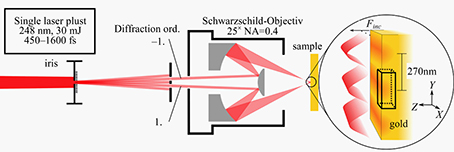
Fig. 1. Mask projection setup for a periodic surface structuring of an area of 40 µm. A sinusoidal interference pattern with a period of 270 nm is obtained by using only the ± 1st diffraction orders (a). Schematic shape of the incident fluence distribution (Finc) created by an ideal single laser pulse self-interference of two beams under a certain angle (b)
a)
b)
c)
d)
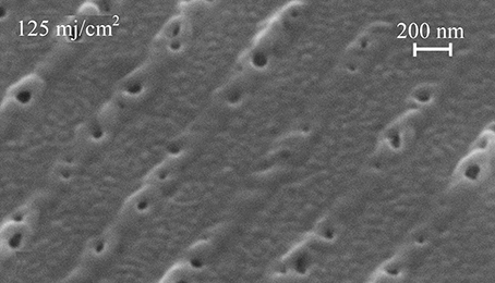
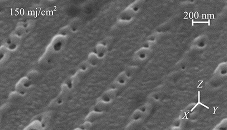
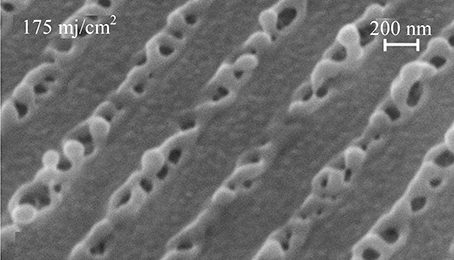
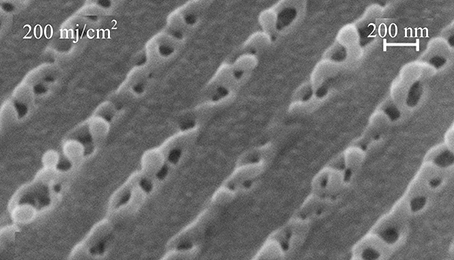
Fig. 2. SEM pictures showing surface modifications from a single laser pulse with periodic line spacing of 270 nm corresponding to the periodic irradiation pattern created by two beam interference for the incident fluences of 125 mJ/cm2 (a), 150 mJ/cm2 (b), 175 mJ/cm2 (c), and 200 mJ/cm2 (d). Small segments of a larger structured area on a thick gold sample at four different average incident fluences are shown. The sample was tilted in the SEM by 45° relative to the electron beam axis to increase the contrast.
The figure is taken from Ref. [19].
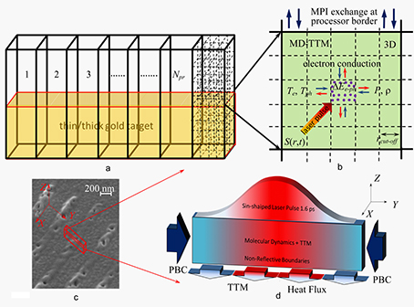
Fig. 3. Schematic representation of the total computational cell divided to the number of processors Nproc (256 in this modeling in Y direction) with utilization of the Message Passing Interface (MPI) library (a). In each processor geometry, a combined atomistic-continuum model MD-TTM was realized in 3D-space (based on cut-off distance of the interatomic potential rcut-off ) subject to find the temperatures of electrons Te and phonons Tph, pressure P, and density ρ for a given laser source S(r,t), where r is the position in space and t is time. The energy exchange between electrons and phonons ∆Ee-ph is accounted for in the model each MD time step. (b). SEM picture (Fig. 2, a) of periodic nanostructures on Au (c) and schematic representation of the computational cell used in the super large scale modeling of this process on the experimental scale (d). PBС are the periodic boundaries. The non-reflective boundaries are transparent for the heat fluxes
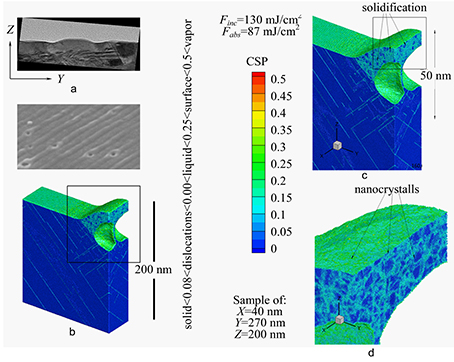
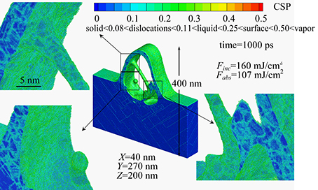
Fig. 4. SEM images of the 270 nm periodic structures (a) with the incident fluence Finc of 130 mJ/cm2 (corresponding to the absorbed fluence Fabs of 87 mJ/cm) are directly compared with the result of an atomistic simulation of the nanostructuring process (b). The atoms are colored with Central Symmetry Parameter (CSP) for distinguishing the atoms with local order (solid – dark blue) from those of disordered structures (grain boundaries – blue, liquid – light blue, surface green, and vapor – red). The magnified view of the final internal microstructure is shown in (c) and (d)
Fig. 5. Atomistic snapshots taken at the end of modeling at t = 1000 ps and obtained in simulation of the periodic nanostructuring process of thick Au target at the incident fluence of 160 mJ/cm2 . Similarly to that of Fig. 4, the atoms are colored according to CSP value. A detailed view on the microscopic structure of the internal structures can be seen in magnified boxes
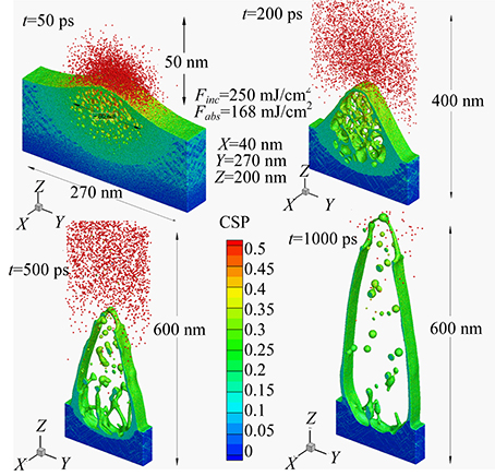
Fig. 6. The sequence of atomic snapshots taken at times 50, 200, 500, and 1000 ps, revealing the dynamics of the nanostructure formation at the fluence 250 mJ/cm2 , that is well above the ablation threshold for Au. The atoms are colored by Central Symmetry Parameter (CSP) parameter
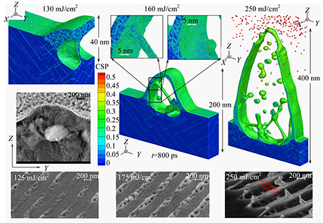
Fig. 7. The obtained in simulations final structures are directly compared [19] with the corresponding experimental SEM images of 270 nm periodic nanostructuring of gold targets with three different average incident fluences shown in columns for 130 mJ/cm2 (a), 160 mJ/cm2 (b), and 250 mJ/cm2 (c). For the case (a), the obtained structure was treated by Focused Ion Beam (FIB) method to prepare a cross section, shown in Transmission Electron Microscopy (TEM) image for visualization of the internal structures in the center of (a). For the case (b), the areas of the atomic snapshot in black rectangles are zoomed for better visualization of the obtained internal polycrystalline structures. The red rectangle on the SEM image in (c) shows the relative position of the computational cell when simulating the nanostructuring process. In all atomic snapshots, taken at the final time of 1000 ps, the atoms are colored according the CSP indicating gaseous atoms (red), surface (green), liquid ambient (light blue), dislocation planes and defects (blue), and the atoms with crystalline surrounding (dark blue)