Abstract
We report low-temperature transport experiments on atomic-size contacts of bismuth that are fabricated using the mechanically controlled break-junction technique at low temperatures. We observe stable contacts with conductance values at fractions of one conductance quantum G0 = 2e2/h, as is expected for systems with long Fermi wavelength. We defer two preferred conductance scales: the lower one is in the order of 0.015 G0 and can be attributed to single-atom Bi contact, while the higher one amounts to 0.15 G0, as indicated by the appearance of multiples of this value in the conductance histogram. Rich magneto-transport behaviour with significant changes in the magneto-conductance is found in the whole conductance range. Although for the pristine samples and large contacts with G > 5 G0, indications for Shubnikov-de Haas oscillations are present, the smallest contacts show pronounced conductance fluctuations that decay rapidly when a magnetic field is applied. Moreover, large variations are observed when a finite bias voltage is applied. These findings are interpreted as the transition from the diffusive to the ballistic and the ultra-quantum regime when lowering the contact size.
Export citation and abstract BibTeX RIS

Content from this work may be used under the terms of the Creative Commons Attribution 3.0 licence. Any further distribution of this work must maintain attribution to the author(s) and the title of the work, journal citation and DOI.
1. Introduction
Metallic atomic contacts have been intensively studied during the last 20 years, not least because they lend themselves to exploring fundamental concepts of nanophysics and quantum transport [1]. Their transport properties are described by the Landauer formula G = G0ΣnTn with the transmission coefficients Tn of the conduction channels, the conductance quantum G0 = 2e2/h, where e is the elementary charge and h is Planck's constant [2]. As a rule of thumb, a single atom contact of a metal accommodates a number of conduction channels that correspond to its chemical valence [3] with transmission coefficients given by the local band structure and the atomic arrangement. The transmission coefficients have been found to saturate at the maximum value Tn = 1, in particular for monovalent metals [1]. As a result the conductance of atomic-size metal contacts may show discrete changes of the conductance in multiples of G0 if atoms are added to the cross section of the contact.
Because both the atomic distance in a crystal and the Fermi wavelength λF of metals amount to a few Ångströms, a nanowire as thin as one atom may act as an electron waveguide with excellent transmission properties. The nanowire is expected to show a conductance described by the Sharvin formula for a cylindrical contact, which in its simplest form, reads GSh = G0 (kFR/2)2 ~ G0, where R is the radius of the nanowire and kF is the Fermi wave vector [1]. However, due to the coincidence of atomic size and Fermi wavelength, structural effects may conceal the waveguide properties of atomic contacts [1] because changing the diameter of the wire by one atom also changes the number of well-transmitted modes by one or a few. Consequently, atomic-size contacts and nanowires of the elementary semimetals are of particular interest because their Fermi wavelength λF  10–50 nm exceeds the atomic size significantly [4]. In these materials, cross-section changes of one atom should give rise to conductance steps that are much smaller than G0 and do not necessarily change the number of transmitting channels. A single-atom contact of a semimetal is expected to show a conductance much smaller than G0, which scales with the ratio between contact size and λF, as described by the Sharvin formula. Although single-atom contacts of Sb reveal a conductance of GSb ~ 0.01 G0 in good agreement with this expectation [5], the situation for Bi is less clear. In some experiments, quantized steps with amplitude G0 have been found [6], while others revealed sub-quanta steps [7] or both quantized steps and sub-quantum steps [8, 9]. There is no apparent correlation between these findings and the experimental methods, which include scanning tunnelling microscope-based techniques [6, 8, 9], mechanically controlled break-junctions [5], or electromigration [7]. The appearance of quantized conduction steps has recently been interpreted as the formation of a topologically protected surface state in Bi bilayers when a nanowire is stretched to breakage [9].
However, most studies of atomic-size structures reported so far have been limited to measurement of the linear conductance or a qualitative treatment of the current-voltage characteristics [6]. This is even more surprising, as Bi in both bulk and nanostructures is known to show a large diversity of interesting transport-related phenomena because of the peculiar electronic properties of this element. Due to a slight lattice distortion, bulk bismuth is a semimetal with a very small band overlap between the valence band and the conduction band in the range of 40 meV at 0 K [10–12].
In the bulk, the electron density n is strongly temperature dependent and amounts to n = 3 × 1017 cm−3 at 4 K, which is four to five orders of magnitude lower than for ordinary metals. The electrical conductivity of Bi nanostructures sometimes shows non-monotonic temperature dependence because of a limitation of the mean free path by temperature-independent boundary scattering [13, 14]. The Fermi surface of Bi consists of ellipsoidal pockets for electrons and holes, resulting in effective masses meff ranging from 0.005 m to 1.2 m for the electrons where m is the free electron mass, and from 0.006 m to 0.7 m for the holes [10–12, 15, 16]. Consequently, the Fermi wavelength depends on the band and varies between λF = 14 nm and 70 nm. In any cases, λF is much longer than the diameter of a Bi atom in the lattice d = 0.37 nm. As a result of the peculiar geometry of the Fermi surface, nanostructures of Bi show a variety of different electronic properties sensitively depending on the size, the shape and the atomic order of the structure [7, 17]. Recently large band-gap fluctuations were observed in Bi nanoparticles by STM measurements [21], pointing towards a close connection between structural and electronic properties. Furthermore, a metal-semiconductor transition and an enhanced thermo-electric figure of merit of Bi nanowires were observed [13–15]. Moreover, granular films of Bi have revealed superconductivity at temperatures as high as 6 K [22].
In the present paper we report magneto-conductance (MC) measurements of atomic-size contacts of Bi with diameters arranging from a single atom up to several atoms. The contacts were produced by stretching a nanostructured thin film of Bi to the breaking point at very low temperatures in cryogenic vacuum, and by carefully closing the gap between the two electrodes again. Our experiments reveal the rich electronic behaviour for which Bi is known [23], including conductance fluctuations [25, 26], Shubnikov-de Haas oscillations [27–29], and quantization effects [1].
2. Experimental
We use the standard techniques of electron-beam lithography, metal evaporation and lift-off to pattern a bismuth stripe (thickness 600 nm) featuring a constriction [30, 31]. By design, the width of the constriction varies linearly from 1 µm down to 100 nm. As substrate we use a gently polished bronze plate covered by a 2 µm thick polyimide layer. Note that in contrast to standard MCBJs the samples are not suspended, because the etching procedure was detrimental to the conductivity of the films. However, studies on non-suspended MCBJs of ferromagnetic metals have been performed before and reproducibly demonstrated the formation of stable atomic-size contacts [32]. A scanning micrograph of a sample is shown in figure 1(a). The thickness of the leads is 600 nm, which is reduced to about 200–300 nm in the constriction region. This size reduction is a consequence of a deposition of the material on top of the mask that reduces its width and eventually pinches it off. Thanks to this self-controlled process the mechanical force, upon bending the sample, concentrates on the constricted area and facilitates stretching the nanowire. We performed x-ray diffraction studies to reveal the type of film growth and the crystal quality; see figure 1(c). The two pronounced peaks at 2Θ = 22.5° and 45.8° correspond to the (111) and (222) directions of the nearly cubic structure. It is worth noting that the hole states of the Fermi surface are located in the (111) direction. From the width of the peaks and rocking curves, we determine a correlation length of 90 nm pointing to a columnar texture, as is also apparent in the SEM micrograph along the edge of a slab cut by focused ion beam; see figure 1(b). We report here transport measurements recorded on two nominally identical samples. The samples are mounted in a custom-made, three-point bending mechanism [31, 33] that is thermally anchored to the mixing chamber of a dilution refrigerator.
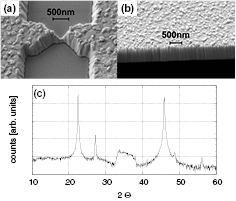
Figure 1. Sample geometry and characterisation. (a) SEM picture of the central part of a sample after measurement. The height of the film in the wide electrodes is 600 nm, which is reduced in the constriction to approximately 200 nm. (b) X-ray scan of a Bi film co-deposited with the sample in panel (a). (c) Cross section of the film of panel (b) cut by focused ion beam. The columnar texture of the film is clearly visible.
Download figure:
Standard image High-resolution imageConductance and MC measurements are performed at low temperatures (30 mK < T < 1 K) in magnetic fields up to 9 T and perpendicular to the sample plane. In order to measure the conductance properties with high resolution in all conductance ranges from a few hundred Ω to the MΩ regime, the sample is connected in series to a calibrated reference resistor of 56 kΩ, which features a very small magnetic-field dependence. The measurement circuit is voltage biased, and the voltage drop across reference resistance and sample are recorded separately to calculate the sample conductance. The transport measurements were performed using a standard lock-in electronic setup with a heavily RF-filtered measurement line in the cryostat. In order to measure the absolute and differential conductance simultaneously, a dc signal was added to the ac modulation of the lock-in amplifier. The AC voltage used for lock-in measurements at the sample was limited to below 3 µV, corresponding to a thermal broadening of 30 mK [33].
3. Results
3.1. Preferred conductance values
The room-temperature resistance of the pristine Bi samples is in the order of 1 kΩ and may slightly increase or decrease towards low temperature; this variation is typical for Bi nanostructures [7, 17]. The breaking curves, i.e. measurements of the conductance as a function of elongation of the bridge, recorded at 4.2 K, reveal no or only very short plateaus at 1 G0, but multiple plateaus at fractions of 1 G0. The exact shape of the individual breaking curves varies from curve to curve as the atomic arrangement changes, but the general shape, e.g. not-very-well-defined plateaus with substructure and curvature, are reproducible [1]. This behaviour is typical for low-temperature measurements in particular, but not exclusively when contacts are formed with the help of lithographic MCBJs [1, 3, 18–20]. Examples of Bi breaking curves are given in figure 2(a), where a pronounced upward slope and curvature of the conductance on the individual plateaus are observed. This behaviour has been reported before for low-temperature measurements on Bi contacts formed in an STM, and explained by a distortion of the lattice and the formation of a metallic-like state with heavy electrons [8]. The transition between the steps is attributed to changes in the atomic configuration that alter the cross-section by one or a few atoms. In contrast to [8], where curved plateaus were found only above G = 0.15 G0, in our samples they also occur reproducibly at conductance values as low as 0.015 G0. Apparently, in our thin-film samples a different metallic-like state can be stabilized. We argue that this state arises from hole transport, because according to the x-ray analysis the <111 > direction hosting the hole states may be aligned with the transport direction. Furthermore, the assumption of hole states naturally explains an increase of conductance within a plateau when stretching it further: the size of the hole pockets at the Fermi surface and their overlap increase when the lattice is elongated. Another example of plateaus with increasing conductance is aluminium [35], which also has hole pocket states at the Fermi surface (there located in the 3rd brillouin zone [34]). In Al, at the plateaus maximum, the saturation transmission of one channel is reached, and it has been suggested that a resonant state develops by the formation of a dimer structure [36, 37]. Because of the small Fermi surface of Bi, such a resonance is not expected to develop fully. However, already a slight distortion of the lattice by the stretching process will gradually increase the band overlap, and thereby enhance EF and the transmission.
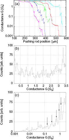
Figure 2. Breaking behaviour. (a) Examples of breaking curves recorded at 4.2 K revealing curved plateaus in abroad conductance range below 1 G0. (b) Linear conductance histogram calculated from 80 opening traces recorded on the same sample. (c) Same data as in panel (b) in logarithmic scale. The arrows indicate conductance plateaus at multiples of G = 0.15 G0.
Download figure:
Standard image High-resolution imageRegardless of the sign of the charge carriers, the observation of these curved plateaus confirms the formation of a metallic-like state, which is formed only in very clean contacts, of a few atoms' size. The metallic character is further confirmed by mostly linear current-voltage characteristics and the observation of quantum-interference effects; see the next section. However, it is not straightforward to determine the conductance of the smallest contact from individual opening traces. We therefore calculate conductance histograms from repeated openings. Figures 2(b) and (c) show conductance histograms calculated from the same 80 opening traces with varying bin size and in different scaling. As a result of the non-suspended sample geometry, smaller bending radii are necessary, and thus the maximum number of opening-breaking repetitions is reduced because often the elastic deformation limit has to be overcome to stretch the wires to rupture. Figure 2(b) shows a linear plot for all data recorded in the range from 0 to 3.5 G0 with a bin size of 0.05 G0. No pronounced peaks are observable at 1 G0 or its multiples. Figure 2(c) shows the same data in a logarithmic conductance scale, revealing broad maxima below 0.1 G0 and several narrower ones between 0.1 and 1.2 G0. The broad maxima at very low conductance arise from the curved plateaus described above. Because within a plateau the conductance may change by a factor of 2 or more, no narrow peaks can be expected. From this histogram we conclude that the smallest stable contacts feature conductance values in the order of 0.02 G0. Figure 2(c) shows several peaks around 0.04 G0,0.07 G0 and 0.15 G0 and its even multiples. The structures at 0.04 G0 and 0.07 G0 are absent in histograms of other samples, and are therefore discarded here. We then consider the peak at 0.15 G0 to be the lowest robust superstructure peak (besides the structures mentioned above around 0.015 G0). We attribute the 0.15 G0 peak and its multiples to somewhat larger, symmetric structures that form, e.g., when crystal planes slide along each other as proposed in [8] and [9]. The fact that the odd multiples are suppressed may indicate bilayer sliding, as suggested in [9]. Due to the film growth with columnar structure, the planes might not develop the topologically protected surface state with perfect transmission, but instead contribute with the smaller value 0.15 G0 to the conductance. Revealing the exact mechanism and origin of these super-structure peaks needs further investigation. We note that the peak at 0.15 G0 is visible in histograms recorded on several samples, although not in all. An alternative interpretation of the data could thus be that the fundamental peak is at 0.3 G0 and all multiples would occur. On the basis of our data we cannot distinguish between these two scenarios. Below, in section 4, we will show that the magnetic field and bias dependence of the transport changes characteristically around 0.2 G0, in agreement with both possibilities.
3.2. Shubnikov-de Haas oscillations
Because of the small Fermi surface of Bi, moderate magnetic fields are sufficient to arrive at the regime where the Fermi body is filled with a small number of Landau levels only [28]. There is a general agreement that for bulk crystalline samples of Bi, when the field is applied along the trigonal axis, the lowest Landau level is driven out of the Fermi surface around B = (8.85 ± 0.2) T-i.e., at the limit of our magnetic field range [23, 24]. For all other orientations this limit is reached at even lower fields. In polycrystalline film samples as they are investigated here, no dependence on the orientation is expected. Figure 3(a) shows two MC curves recorded at a pristine sample for T = 4.2 K and T = 120 mK. In figures 3(b), at (T = 4.2 K) and 3(c) (T = 120 mK) the background MC has been subtracted and the data is plotted versus 1/B separately for both field directions to reveal the high symmetry of the G(B) curves. At T = 4.2 K a sawtooth-like behaviour is observed for both sweep directions of B, while at T = 120 mK no regular pattern arises, but aperiodic conductance fluctuations (CF) govern the pattern. The origin of these CF will be discussed in the next section. The sawtooth pattern is not equidistant in 1/B, as would be expected for Shubnikov-de Haas (SdH) oscillations for a 3D Fermi surface with a constant cross-section [27–29]. However, when approaching the ultra-quantum regime, deviations from the usual functional behaviour are expected, and were indeed observed for Bi single crystals [23, 24]. Here we observe an abrupt increase in the periodicity around 1/B = 0.27 1/T. Since the periodicity of the SdH oscillation is a measure of the extreme cross-sections of the Fermi surface perpendicular to the applied field, this signals a reorientation or reshaping of the Fermi surface at around 4 T. This transition becomes even more apparent when plotting dG as a function of B; see figure 3(d), where we show two subsequent sweeps recorded at 4.2 K, one for increasing and one for decreasing field. A periodic variation of the conductance as a function of B would indicate a physical phenomenon, e.g. the Aharonov Bohm effect, which is related to real space rather than in k space. Also in this scaling, the peaks are not equidistant and one observes a transition from a longer period at low field (|B| < 3.5 T) via a region were two periods seem to be superimposed (3.5 T < |B| < 5.5 T) to a shorter period (|B| > 5.5 T). Although we cannot definitely reveal the physical origin of the periodicity changes, they suggest that the magnetic field, in combination with the low dimension, initiates a reversible structural change in the constriction that gives rise to significant changes in the charge transport behaviour. This interpretation is supported by the observation of a pronounced change in the CF in a similar field range, as we will show in the next section. Although this is a rather unlikely scenario for conventional metals, the extreme sensitivity of the electronic properties of Bi to minor geometrical changes may make this a possible scenario for Bi [50, 51].
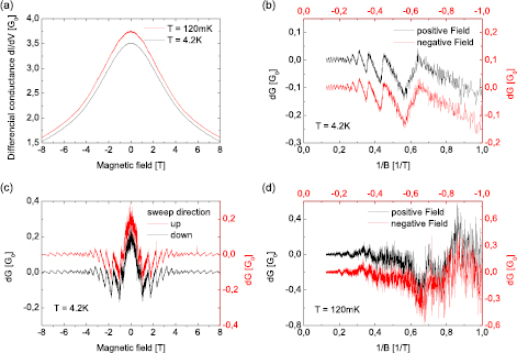
Figure 3. Quasiperiodic magneto-conductance (MC) oscillations. (a) Magneto-conductance of a pristine sample for T = 4.2 K and T = 120 mK. (b), (c) Same data as in (a) after subtraction of the background plotted verus1/B. (b) data for T = 4.2 K, (c) data for T = 120 mK. (d) Two subsequently recorded data sets (after subtraction of background) for T = 4.2 K and inversed sweep directions plotted versus B. The down sweep corresponds to the data set shown in (a) and (b).
Download figure:
Standard image High-resolution image3.3. Conductance fluctuations
We now turn to the description of the magneto-conductance (MC) measurements recorded for selected contacts. As an example, figure 4(a) shows the differential conductance dI/dV versus B of a contact with G(B = 0 T) = 1.38 G0 recorded at T = 150 mK. It shows a bell shape with a plateau region between −1.5 T and 1.5. T and a saturation above |B| = 7 T at G ~ 0.76 G0. The red curve is a moving average calculated over a field range of ΔB = 1 T, which is used for subtraction of the long-range field dependence for analysis of the CF. Figure 4(b) shows the CF signal dG after subtraction; figure 4(c) summarizes the symmetry analysis: for negative field direction we plot the anti-symmetrized part (dG(B) − dG(−B))/2, and for positive field direction, the symmetric part (dG(B) + dG(−B))/2. In a two-point geometry, and if the transport is time-reversal symmetric, the CFs are expected to be symmetric with respect to field inversion [25, 26, 38]. The analysis reveals that this is fulfilled for Bi atomic-size contacts. The remaining anti-symmetric signal shows the characteristics of white noise and reflects the high signal-to-noise ratio of the measurement with a voltage noise that amounts to ~ 1 nV. Figure 4(d) shows the anti-autocorrelation function

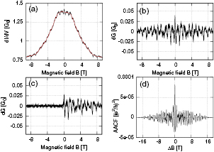
Figure 4. Magneto-conductance (MC) and conductance fluctuation analysis. (a) MC curve of a contact measured at T = 150 mK. It reveals a bell-shape background that is subtracted by a moving averager (red line). (b) MC after subtraction of background. (c) Symmetrized signal revealing the high signal to noise ratio. For positive/negative field direction symmetric/antisymmetric part of the signal (dG(B) ± dG(−B))/2 is plotted. (d) Anti-autocorrelation function of the data shown in (b). The fluctuation amplitude Grms and the correlation field Bc are determined from the maximum of the AACF at zero field difference: Grms = (AACF(ΔB = 0))1/2 and Bc = HFWM (half width at half maximum).
Download figure:
Standard image High-resolution imagefrom which we determine the characteristic properties of the CF-i.e. the fluctuation amplitude Grms is the square-root of the main maximum  , and the correlation field Bc is the half-width at half maximum
  [25, 26, 38]. In the fully phase-coherent diffusive regime for metals with strong spin-orbit scattering, a universal amplitude of Gucf = 0.25 G0 is expected [25, 26, 38].
Figure 5 summarizes typical MC curves recorded when stretching a sample starting at roughly 5 G0 down to 0.014 G0. The bell-shaped background MC is subtracted and the traces are offset for clarity; the zero-bias conductance (ZBC) values for each trace are indicated in the legend. The most prominent observations are as follows: for high conductance there is a pronounced peak around zero-field that diminishes with decreasing conductance and is indistinguishable from the CFs below ZBC of 0.2 G0. We attribute this peak to weak antilocalization, as is expected for elements with high atomic numbers and therefore high spin–orbit coupling [39–41]. The analysis of the fitting to the 1D theory [40, 41] yields a rough estimate for the phase coherence length lϕ = 150 nm for contacts above 1 G0. This value is somewhat smaller than the findings by Rudolph and Heremans [42] on Bi wires patterned from thin films, who observed a width-dependence of lϕ. We note that our data could not be described with the 2D formula (as was used in [42]), which indicates that in our experiment lϕ was limited by the sample geometry rather than by intrinsic length scales. Also, the disappearance of the antilocalization peak for the contacts with very small conductance hints towards geometry limited transport phenomena. In this sense the obtained value for lϕ represents a lower limit. This analysis also indicates a lower diffusion coefficient in our columnar films than the smooth films investigated in [42].

Figure 5. Differential conductance as a function of magnetic field after subtraction of the background for several contacts of the same sample measured at T < 150 mK, revealing aperiodic, but reproducible conductance fluctuations. The traces are offset for clarity. The zero-bias conductance dI/dV(0) for each trace is indicated in the legend. The amplitudes of the two lowest traces (for the smallest dI/dV(0)) have been multiplied by 10.
Download figure:
Standard image High-resolution imageFor the analysis of the CF the zero-field peak is cutout of the calculation of the AACF because the integration range is normalized accordingly to obtain the correct CF amplitude. The amplitude of the CF diminishes with decreasing G, so the lowest two traces in figure 5 have been multiplied by 10 for better visibility. We also note that for contacts above 1 G0, the fluctuation amplitude is considerably reduced for magnetic fields above |B| > 3 T. This indicates a change in the trajectories that contribute to the interference pattern. In combination with the results from the SdH oscillations described above, we suggest a change of the transport mechanism above this field range. For the further analysis we calculated the anti-autocorrelation functions of all CF traces and determined the rms amplitude Grms and the correlation field Bc from its main maximum, as described above [25, 26]. Figure 6 shows the results of 35 contacts investigated in the same sample, at similar temperature T < 150 mK. The amplitude Grms increases steadily from very low values Grms << 0.001 G0 at low conductance and levels off to roughly Grms ~ 0.025 G0 at around 3 G0, with rather large standard deviation. Also, this saturation value is one order of magnitude smaller than expected for universal conductance fluctuations in the diffusive regime [25, 41]. A reduction of the CF was reported for ballistic metal contacts [43], and is explained by a reduced probability of the charge carriers being scattered back through the constriction and contributing to the interference pattern Grms/GUCF ~ l/a. For Bi, with its very long λF and its medium elastic mean free path l, this ratio is very small, and an even smaller amplitude Grms could be expected here. The same reduced backscattering probability may explain the reduced antilocalization peak for the smallest contacts. Similarly, it has been shown for atomic contacts of noble metals that the CF amplitude as a function of bias is connected with the interference of electronic trajectories being backscattered from the atomic contact and those being backscattered from the reservoir [44]. This means the CFs of atomic-size contacts are sensitive to the local structure at the contact region itself. When the transmission probability of the contact is small, the fluctuation amplitude is strongly reduced. A quantitative comparison between the model of [44] and our experiment cannot be made because of the complex Fermi surface of Bi.

Figure 6. Analysis results, Grms and Bc, of the conductance fluctuations of 35 contacts measured at the same sample at T < 150 mK.
Download figure:
Standard image High-resolution imageThe correlation field Bc shows no discernible trend. Within the numerical uncertainty range it is constant <Bc > = 90 mT ± 10 mT. Bc describes the typical averaged 'period' of the aperiodic fluctuations. It is a measure for the length of the electronic paths that contribute to the fluctuation pattern. When the sample is a 2D plane, Bc is translated into an effective path length by l2D = (h/eBc)1/2. For wire-shaped samples with width w smaller than the effective length, it has to be calculated according to: l1D = h/eBcw [41]. While in ballistic metal contacts, the phase area contributing to the CF is given by the temperature-independent elastic mean free path l [43]; in the diffusive limit it is given by the minimum of either the thermal length lT = (hD/kBT)1/2 or the phase coherence length lϕ. [25, 26, 41]. However, this has only been worked out quantitatively for systems in which λF is much shorter than l and which, in turn, is shorter than lϕ.. Since for our samples the 2D analysis yields l2D = 220 nm > w = 120 nm, the 2D approximation is not valid and we have to apply the 1D formula, from which we obtain l1D ~ 480 nm. This value is higher than the lower estimate for lϕ that we obtained from the weak localization analysis above, but larger than the crystal grain structure and the film thickness in the contact area that limit the elastic mean free path. The physical meaning of this length can be revealed by temperature-dependent measurements. Up to our highest measurement temperature of 1 K, the fluctuation amplitude, as well as Bc, showed only a very weak variation (not shown). We therefore assume that temperature averaging is not the limiting quantity in our experiment. We conclude that l1D has to be identified with lϕ, which determines the dominating interference paths of the CFs as for diffusive wires. However, because the theory of CFs has not been developed for the unusual combination of length scales and because of the limited temperature range of our cryostat, we cannot certainly conclude on the physical meaning of the effective length.
3.4. Bias-dependent measurements
To get further inside the transport mechanism, we performed bias- and magnetic field-dependent measurements of the differential conductance. Figure 7 shows typical dI/dV(B,V) maps of eight contacts ranging from dI/dV(0,0) = 0.013 G0 to 3.022 G0; selected traces from the two lowermost panels are shown in figure 8. Pronounced variations of G are observed as function of the bias and as function of the magnetic field. They are reproducible when repeating the bias or field sweep, respectively. The CFs are not symmetric with respect to bias inversion in agreement with theory and earlier observations [25, 38, 41, 40]. In addition, we observe the excitation of temporal fluctuations at higher bias levels that give rise to non-reproducible traces and showup in figure 8 as an increased noise level. To distinguish these three effects, we denote the fluctuations as function of bias as CFV, the fluctuations as function of magnetic field as CFB, and the temporal fluctuations as CFt.
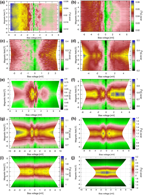
Figure 7. Differential conductance dI/dV as a function of applied magnetic field and bias voltage for a selection of eight contacts of the same sample, measured at low temperature T < 150 mK. The conductance at zero field and zero bias (dI/dV(B = 0, V = 0)) in the left panels are from top to bottom: 0.013 G0, 0.03 G0, 0.3 G0, 0.65 G0 and in the right panels from top to bottom: 0.9 G0, 1.2 G0, 1.6 G0, and 2.8 G0.
Download figure:
Standard image High-resolution image
Figure 8. Selected traces taken from the two lowest panels of figure 7 revealing the excitation of fluctuations at high bias. (a) for dI/dV(0,0) = 2.8 G0 and (b) dI/dV(0,0) = 0.65 G0. In panel (b) the races have been offset by multiples of 0.15 G0 with respect to the trace recorded at B = 0.
Download figure:
Standard image High-resolution image
The amplitude of the CFV is reduced when applying higher bias or higher magnetic fields. The field scales at which the reduction becomes apparent depends on the contact size and the applied field. The reduction with magnetic field is in agreement with the observations described above (figure 5). It indicates a loss of phase coherence or reduction of interference path with increasing field, while the reduction of the CFV amplitude with increasing bias indicates loss of phase coherence due to smearing of the Fermi edge [40]. Alternative explanations, such as inelastic excitations of phonons [52], can be excluded because these would give rise to symmetric features with respect to bias reversal.
The CFt signal sets in at higher bias level when the CFV signal is already reduced. We attribute these fluctuations to atomic rearrangements caused by joule heating in the constriction area, although the currentdensity is still relatively low compared to typical currentdensities known to exert atomic fluctuations [45–47]. This interpretation is supported by the occasional occurrence of conductance jumps (see the four topmost curves in figure 8(b)), as has been found for single-atom junctions [37]. In most cases, however, the CFt amplitudes are small and occur around a constant mean conductance value. This means that the atomic motion seems to be limited to small variations around their stable positions. Exceptions are given by the curves recorded at B = 1 T and B = 3 T in figure 8(b), where small, irreversible changes are observed. Due to the particular sensitivity of the electronic properties of Bi to small changes of the crystal structure, spatially small variations might also give rise to pronounced changes of the conductance [48–51]. Both the CFV and the CFt amplitudes are reduced above around |B| = 4 T, indicating that the origin of the CFt is also field dependent. In other contacts (not shown here), the CFt amplitude may increase with increasing magnetic field. Such interplay between bias, magnetic field and two-level fluctuations has been observed in mesoscopic Bi samples [49, 51] and was interpreted as originating from field-dependent local double-well potentials created by structural defects. In the samples investigated here, the CFt do not show a clear two-level structure, presumably because several fluctuators are active. Summarizing this part, we argue that the temporal fluctuations are caused by changes of the electronic interference paths because of dissipation-induced small-scale motion of atoms. They are modulated by the magnetic field because the field affects the phase of the electronic waves. We now discuss the dependence of the CFs on the zero-field conductance. Although for small conductance G < 0.2 G0 the magnetic field dependence CFB is much smaller than the bias dependence CFV, it is opposite for larger conductance. An intermediate regime where field- and bias dependence are of comparable order of magnitude is found in a range from 0.15 to 0.8 G0. The suppression of the magnetic field dependence CFB for small contacts is in agreement with a transition from diffusive to ballistic transport: The origin of the pronounced negative MC (i.e. positive magnetoresistance) is the orbital magnetoresistance-i.e. the effective reduction of the mean free path, when the paths of the charge carriers are deflected by the Lorentz force [53]. When the lateral size of a wire becomes comparable to or smaller than the elastic mean free path, this effect is suppressed [54].
4. Conclusions
Summarizing, we report a comprehensive study of the magneto-conductance of atomic-size Bi contacts fabricated by the mechanically controlled break-junction technique. The transport behaviour changes twice, at around 0.015 G0 and at 0.15 G0. We observe conductance fluctuations that the charge transport is phase coherently over a length scale of 100 nm or more. Furthermore, we find indications for structural changes when the magnetic field exceeds a few Tesla. This structural transition change may go along with a change in the dominating carrier species-i.e. from hole to electron transport. Further measurements, e.g. of thermo power or Hall effect in strained thin films, would be required to clarify this issue.
Acknowledgements
We thank C Debuschewitz, C Schirm, V Kunej and C Bacca for valuable and fruitful discussions about this work and for their contributions in the early state of the experiments. We are grateful to A Liebig for performing the x-ray diffractometry. We acknowledge experimental and technical assistance of A Fischer. We gratefully acknowledge financial support from the Krupp foundation and from the Baden-Württemberg-Stiftung in the framework of the Research Network Functional Nanostructures.
Author Contributions
HFP fabricated the samples constructed the experimental set-up and performed the measurements. ES initiated the project, and ES and TP wrote the manuscript. All authors analyzed the data and discussed the results. All authors have given approval to the final version of the manuscript.
Funding Sources
The project was financially supported by the Alfried-Krupp von Bohlen und Halbach foundation and by the Baden-Württemberg foundation.